
![]()


|
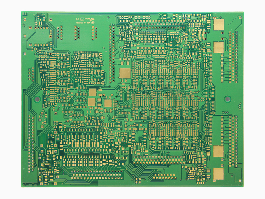
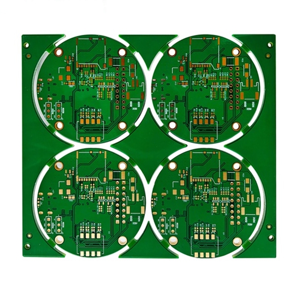
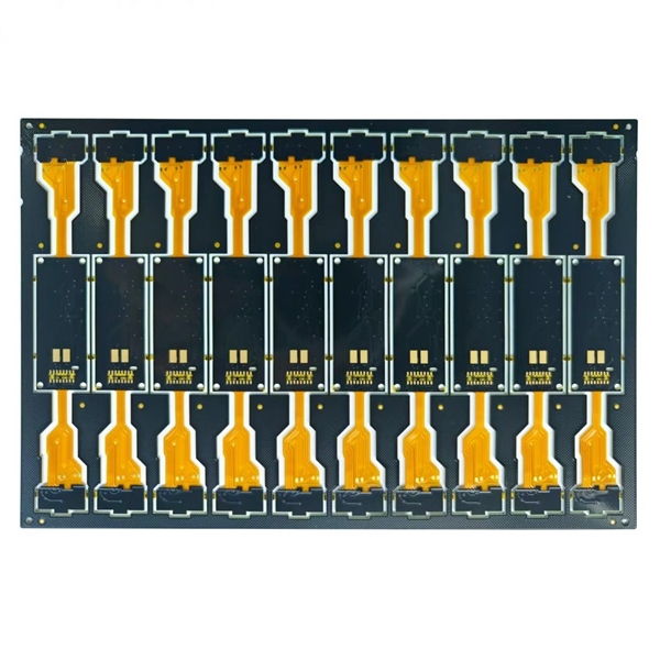
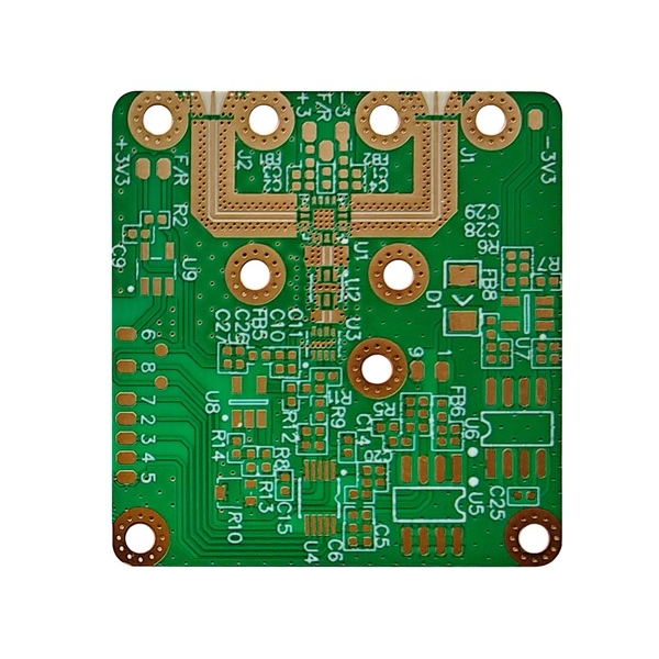
PCB Capabilities |
|
|
Min. PCB Dimension |
Min. 5*5*0.3mm |
|
Max. PCB Dimension |
1200*650mm |
|
PCB Material |
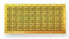
CEM-1, CEM-3, FR4, Rogers, Al base, FPC, Ceramic |
|
PCB Surface Finish |
HAL Lead-free HASL, Falsh Gold, ENIG (Immersion Gold), OSP(Entek), Immersion Tin, Immersion Silver, Hard Gold, ENEPIG |
|
Chip & IC size |
Min. 0201(0.5*0.25mm) Max. 55mm |
|
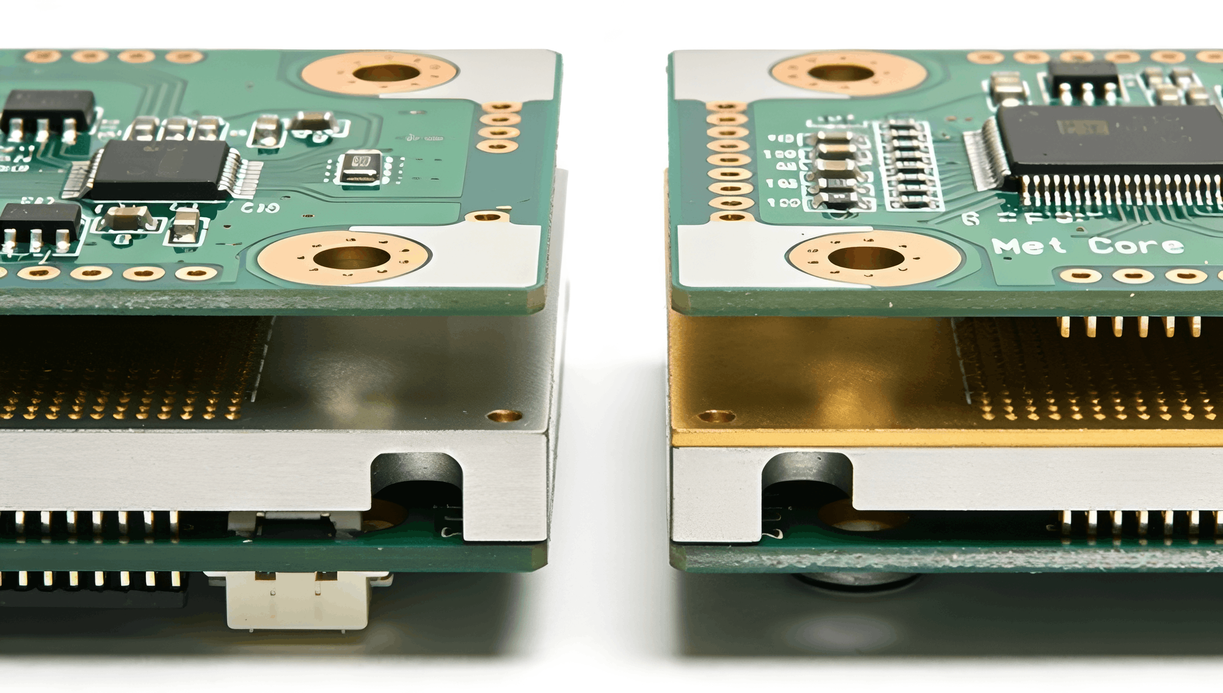
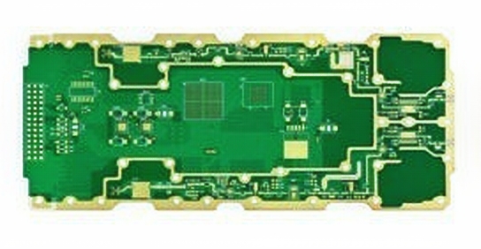
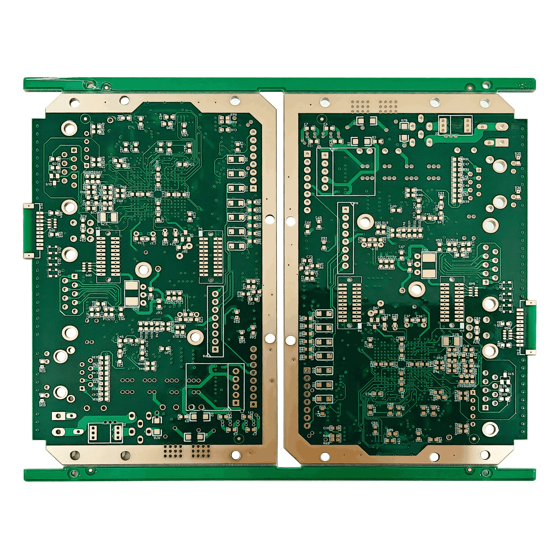
Layer |
1 - 32L |
|
Copper Thickness |
Min. base copper: 1 / 4Oz |
|
Max. base copper: 6Oz |
|
|
Max. Aspect Ratio |
12 : 01mm |
|
Hole Size Tolerance |
±0.075(PTH) ±0.05mm(NPTH) |
|
Min. Hole Size |
0.1mm |
|
Min. BGA Size |
0.2mm |
|
PCB type |
Normal through hole, HDI PCB, High Frequency, Buried and Blind vias PCB |
|
PCB Electrical Testing |
Flying probe testing, E-testing jig, Automotic E-testing line |
Leadtime of Tenpoint PCB orders:
|
TH PCB |
/days |
|||
|
Type |
Samples |
Mass Production |
||
|
Normal |
Expedited |
Normal |
Expedited |
|
|
Single Layer |
4 |
2 |
7 |
3 |
|
Double layer |
6 |
2 |
8 |
4 |
|
4 Layer |
7 |
3 |
9 |
5 |
|
6 Layer |
8 |
3 |
10 |
6 |
|
8 Layer |
10 |
5 |
12 |
8 |
|
10 Layer |
12 |
8 |
15 |
10 |
|
HDI PCB |
/days |
|||
|
Type |
Samples |
Mass Production |
||
|
Normal |
Expedited |
Normal |
Expedited |
|
|
4 Layer |
10 |
6 |
13 |
8 |
|
6 Layer |
12 |
7 |
14 |
9 |
|
8 Layer |
15 |
9 |
17 |
12 |
|
10 Layer |
17 |
11 |
19 |
13 |
If there is extra special requirements like expoxy filled, peelable mask, the leadtime will be longer.
QUICK GUIDE
SHIPPING METHOD

LEAVE YOUR MESSAGE